Prelims: Current events of national and international importance | Science and Technology
Why in News?
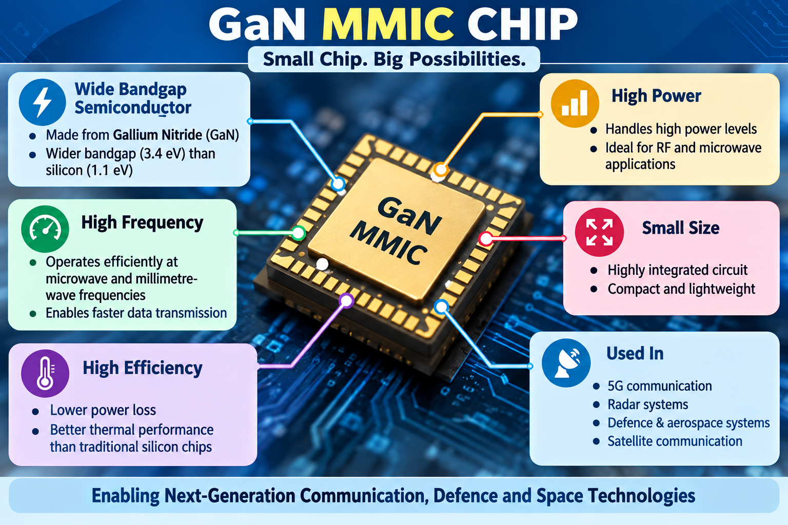
The Defence Research and Development Organisation (DRDO) has successfully demonstrated and implemented indigenous Gallium Nitride (GaN) Monolithic Microwave Integrated Circuit (MMIC) technology.
GaN MMIC Technology
- Gallium Nitride (GaN) - A wide-bandgap semiconductor material superior to traditional Silicon (Si) and Gallium Arsenide (GaAs) for high-frequency and high-power applications.
- MMIC (Monolithic Microwave Integrated Circuit)- An integrated circuit device operating at microwave frequencies (300 MHz to 300 GHz), combining active functions (amplifiers, switches) onto a single semiconductor substrate.
- Performance Benchmark- A single indigenous GaN chip measuring just 3.5 mm×3 mm delivers up to 30 Watts of power.
- It operates at speeds up to 300 times faster than conventional silicon.
- India joins an elite group of nations, including the US, Russia, France, Germany, South Korea, and China possessing native GaN MMIC design and fabrication technology.
Key Technical Highlights
- Developed primarily by - DRDO’s Solid State Physics Laboratory (SSPL) in New Delhi, with pilot production capabilities established at the Galium Arsenide Enabling Technology Centre (GAETEC) in Hyderabad.
- Frequency Coverage
- S-Band- Designed, fabricated, and demonstrated S-band GaN High Electron-Mobility Transistor (HEMT) power bars, Power Amplifiers, Low Noise Amplifiers (LNA), and switch MMICs.
- X-Band - Successfully demonstrated and implemented GaN MMIC technology for applications extending up to the X-band (8 to 12 GHz).
- Substrate Technology - Built using indigenous processes for growing and manufacturing 4-inch diameter Silicon Carbide (SiC) substrates (GaN-on-SiC), providing exceptional thermal dissipation.
Strategic Applications
- Next-Generation Radars - Transmit/Receive (T/R) modules powered by GaN MMICs generate significantly higher RF output power, expanding detection ranges, enhancing target tracking, and shrinking physical array sizes in Active Electronically Scanned Array (AESA) radars.
- Electronic Warfare (EW) - Enhances airborne and naval EW jammers capable of generating high-power directional jamming signals across wide bandwidths to blind hostile radar networks.
- Space & Guided Missiles - Provides high-power density, thermal tolerance, and radiation hardness for compact radar seekers in precision-guided missiles and satellite communication (SatCom) payloads.
- Strategic Autonomy - Eliminates critical reliance on foreign imports and bypasses Western denial regimes/export-control restrictions (such as ITAR) governing high-end semiconductor components.
Reference
Economic Times | GaN technology